2D Examples
Magnetron discharge simulation with A700V chamber layout
We performed a series of quasi two-dimensional magnetron discharge simulations in argon. Hereby we used a simplified chamber layout of our A700V coater to define the simulation domain. The results were a little bit puzzling, cause they do not match with oberservations and/or measurements on our real coater. It seemed there is anything wrong or missing in the simulation setup or in our software. Hence, we tried to figure out the problem using a well defined parameter set. The simulation parameters can be found in the table below. If not mentioned otherwise these are settings the following simulation results are based on.
| Parameter | Setting | Unit |
|---|---|---|
| Argon pressure | 0.5 | [Pascal] |
| Applied power | 100 | [W/m] |
| Chamber wall potential | 0 (grounded) | [V] |
| Dark space shield spacing | 1 | [mm] |
| Electron time step | 2.5e-11 | [s] |
| Cell spacing | 1 x 1 x 1 | [mm3 ] |
| Charge weighting | 5e5 | [-] |
| Secondary electron yield | 0.088 (argon on copper) | [-] |
| Electron scattering | isotropic | [-] |
| Electron energy partitioning | one-takes-it-all | [-] |
| Electron reflection on wall | None | [-] |
Table 1: PIC-MC settings and simulation parameters used for the DC magnetron discharge simulations.
We tried out two kinds of magnetron configurations for the general PK750 magnetron design, i.e. balanced and unbalanced, respectively. The balanced magnetron configuration uses the same size and strength for the inner and outer magnets on the yoke. For the unbalanced configuration however, size and/or strength can differ either for the inner or outer magnets, whether one wants more or less ion bombardment on the substrate. In the figures below you see the magnetic isolines for the balanced and unbalanced magnetron configuration, respectively.
| Inner remanence = outer remanence = 1.35 | Inner remanence = 0.85, outer remanence = 1.35 |
|---|---|
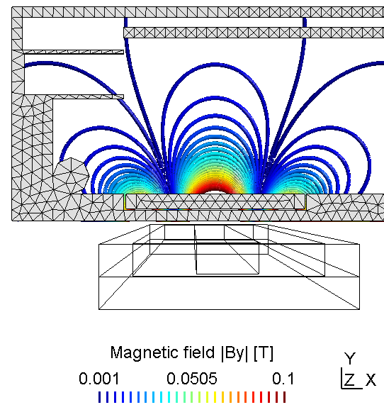 | 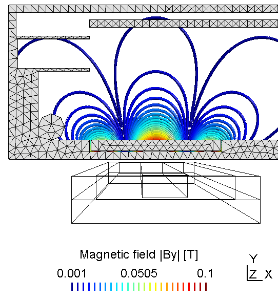 |
Figure 1: Isolines of the magnetic field strength in y-direction for the balanced (left) and unbalanced (right) magnetic configuration.
Unbalanced magnetron: Anode shielding with substrate on floating potential
In this simulation we used the unbalanced magnetron configuration. With an unbalanced magnetron however, it seems the plasma is more sensitive to the anode configuration. Whereas the left plasma is conductively connected to the ajacent chamber wall, the right one is connected with the top of the chamber wall. Thus, with the substrate on floating potential some of the anodic surface is shielded causing the right plasma to fade (fig. 1). With the substrate on ground potential however,the right plasma is as bright as the left one (fig. 2) due to an anodic surface to connect with.
Due to the uncoupled electron drift current in a 2d setup this effect is even more pronounced. Thus, if using constant power the voltage can drop below ignition point causing the right plasma to diminish.
| Substrate on floating potential | |
|---|---|
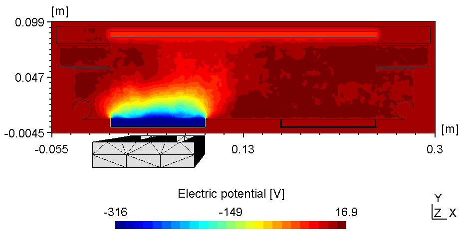 | 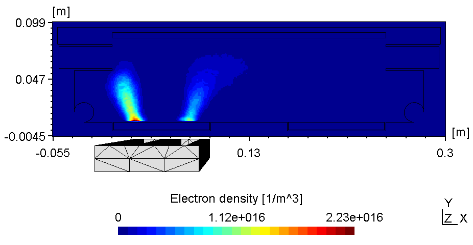 |
Figure 1: Electric potential (left) and electron density (right) during simulation with substrate on floating potential.
| Substrate on ground potential | |
|---|---|
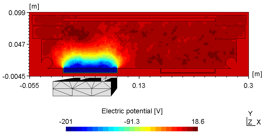 | 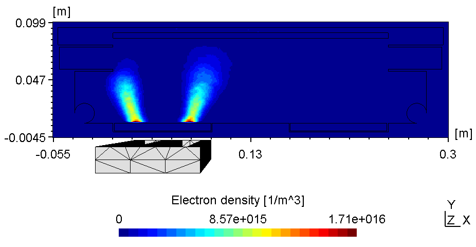 |
Figure 2: Electric potential (left) and electron density (right) during simulation with substrate on ground potential (0 V).
Balanced magnetron: Short-circuit with dark space shielding
As seen in the pictures below we get some anomalies if using our coater geomtry settings together with a balanced magnetron. A spacing of 1 mm between target and dark space shielding causes an distortion of the electric field. Thus, we get an extensive electric field strength parallel to the target surface. Thus, electrons are shifted sideways in the magnetic confinement and can escape more easily. Therefore excessively high voltages are needed to get a self sustaining plasma which is even so quite unstable.
| Short-circuit with the edge of the dark space shielding | |
|---|---|
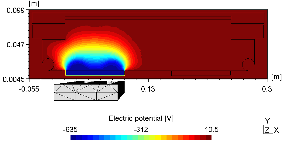 | 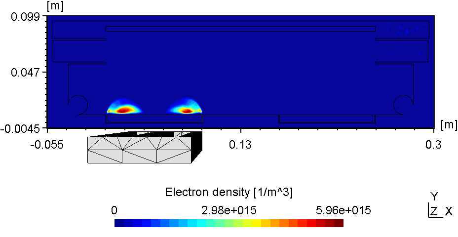 |
Figure 1: Electric potential (left) and electron density (right) during simulation with balanced magnetron.
| Short-circuit with the edge of the dark space shielding | |
|---|---|
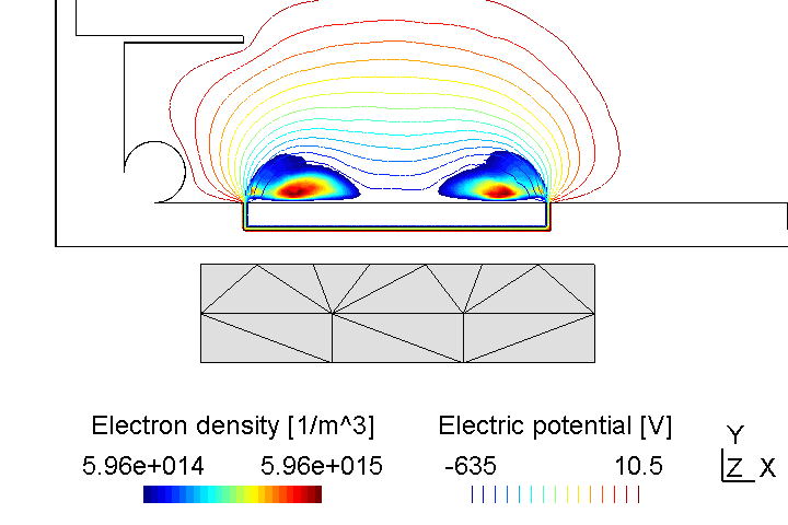 | 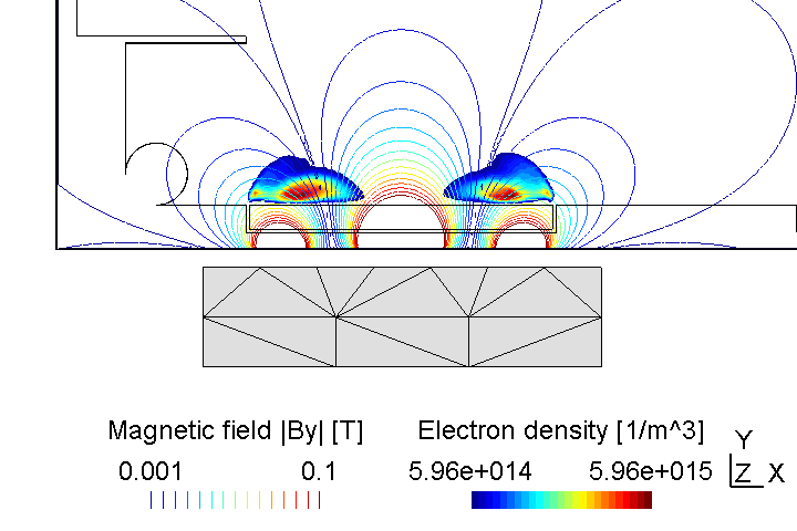 |
Figure 2: Electron density overlayed with electric potential (left) and magnetic field By (right) isolines.